|
preface
|
introduction
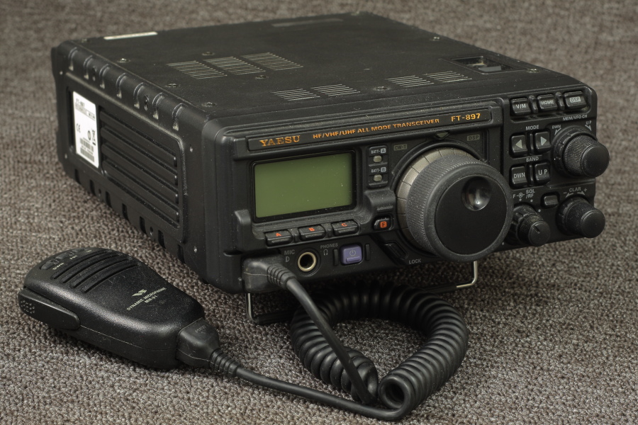
The FT-897 was approved by the FCC on May 9, 2002 and has been in production since then until 2016. This FT-897 is the "big brother" of the FT-817 transceiver introduced two years earlier. The big difference is the transmit power and for the rest the transceivers are largely similar. It is a solid HF + 6 + 2 + 70 all-mode mobile transceiver. The set is nicely compact and has all basic functions and can generate 100 Watts on HF and 50 Watts on VHF. Given the low power consumption, the set is perfect for field work. Two batteries or a switched power supply can be installed.
personal introduction
The Yaesu FT-8x7 series is a series of radios that I have a soft spot for. The 817, 857 and 897 have been in possession. Due to shifting equipment and budgets, radios have come and gone. Initially I made most of the radio connections with the FT-897D, but due to an upgrade to an FT-991, the FT-897D and FT-857 were sold at the time. In retrospect I regret this because the FT-991 is not "my radio". Hence the FT-991 has been sold and replaced by an Icom IC-7300 for HF. An FT-897D has been bought back for fieldwork and V / UHF. I don't dare to put an expensive IC-7300 in a damp tent during field days and then an FT-897D is a good candidate. In addition, an FT-897D is an all-in-one radio that is "good for everything"
The FT-897 (D) is one of the most characteristic sets of our time for me. There is already a successor in the form of the FT-991, but the FT-897 (D) remains my favorite. There are newer techniques such as band scopes and better noise reduction, but the FT-897 (D) remains very interesting in 2018.
shack in a box
Most importantly, it is a "shack in a box". This set can receive and transmit on the amateur bands from 160 m to 6 meters, 2 meters and 70 cm! Most sets are HF or V / UHF where this set has "everything". Unfortunately the recently released 4 meter band is not there due to an "unfortunate chosen" mixing frequency.
power consumption
One of the advantages of the FT-897 is that the design is quite basic and therefore consumes relatively little power. When received, the set consumes about 700 mA with the newer FT-991 already consuming 2 A. The new signal processing techniques are realized in microchips that consume quite a lot of power. So the FT-897 is perfect for use in the field (on battery). In addition, there is a lot of ambient noise in the field, which makes the lack of noise reduction less relevant.
|
|
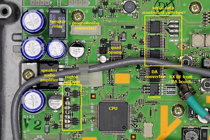
CPU / EEPROM
|
CPU
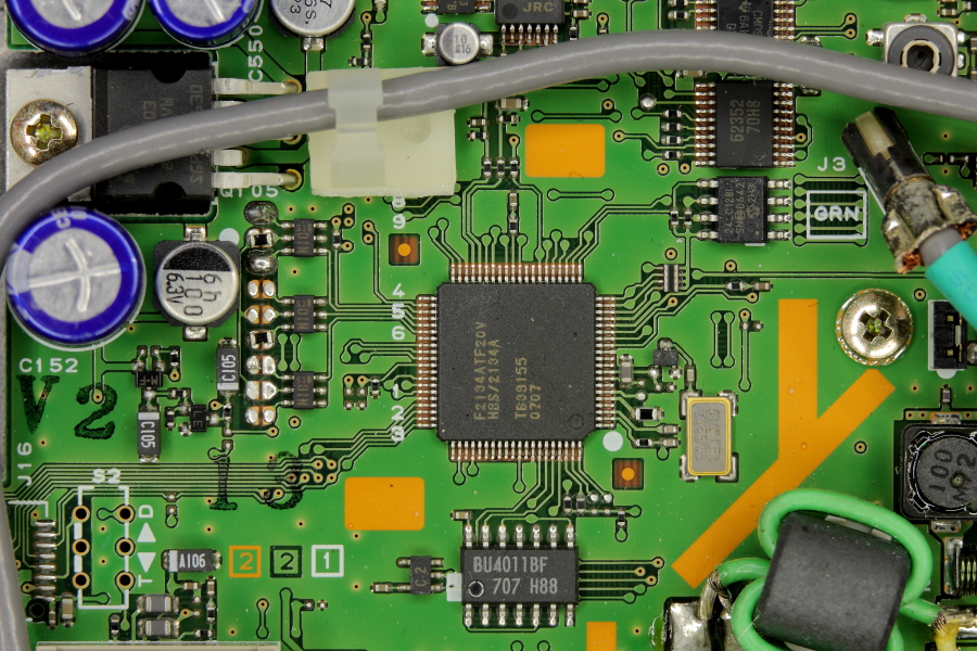
The "beating heart" of the set is a microprocessor (CPU: Central Processing Unit) that controls all processes. The "black stamp" is clearly visible in the photo below.
EEPROM
A 128 kb EEPROM is visible above the CPU. When starting the set, the settings and parameters are read by the CPU. When closing the set, the changes in the set are written to the same EEPROM . Channel information such as frequency, subtone and label is stored in the EEPROM. Also parameters such as the sweep setting, transmit power and other calibration data. Digital data can be converted into an analog voltage via digital / analog converter chips. These voltages are used to generate analog voltages (via opamps). These analog voltages can be reference voltages for surrounding circuits. When replacing this EEPROM, the set must therefore be fully adjusted.
Nine solder pads are visible to the left of the CPU. The white text next to it (in remarkable order) indicates the identification of the "solder pads" . Connecting or disconnecting here can affect the CPU program. With this you can change region settings. For example, the band restriction can be specified so that it can also be sent outside the amateur bands. This can be useful to use amateur bands that were not originally available or to use the set as a continuous signal generator. Fortunately, risky bands, such as the broadcasting basket and the aviation band, are always blocked.
oscillator
To the right of the CPU is a crystal oscillator . This crystal provides a clock frequency for the CPU. Because the generated frequency (19.82 MHz) could interfere with a receiving frequency, it is possible to adjust the clock frequency slightly. The CPU can send a signal to a transistor that couples an additional capacitor to the crystal oscillator. By adding this capacity, the clock frequency is "shifted" slightly. This "Clock Shift" can be turned on or off via the menu.
version designation
At the bottom left of the photo you can see three numbers in a box. This is the version marking of the print. The left "2" indicates that the etching pattern of the print is version 2. The second "2" indicates that the green soldermask is version 2. The right "1" means that the white zwwprint text on the print is version 1.
|
|
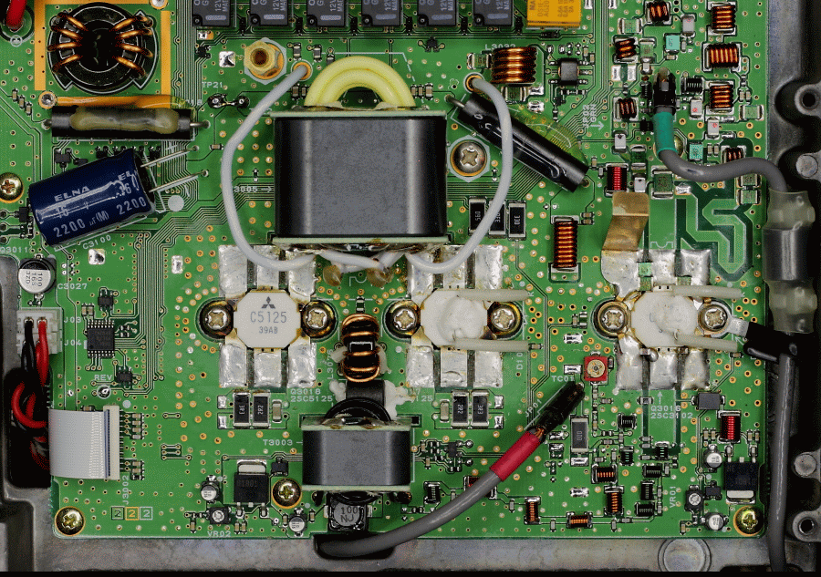
power amplifier driver
|
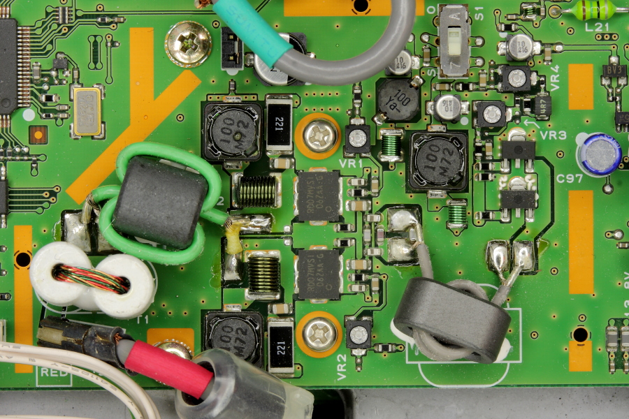
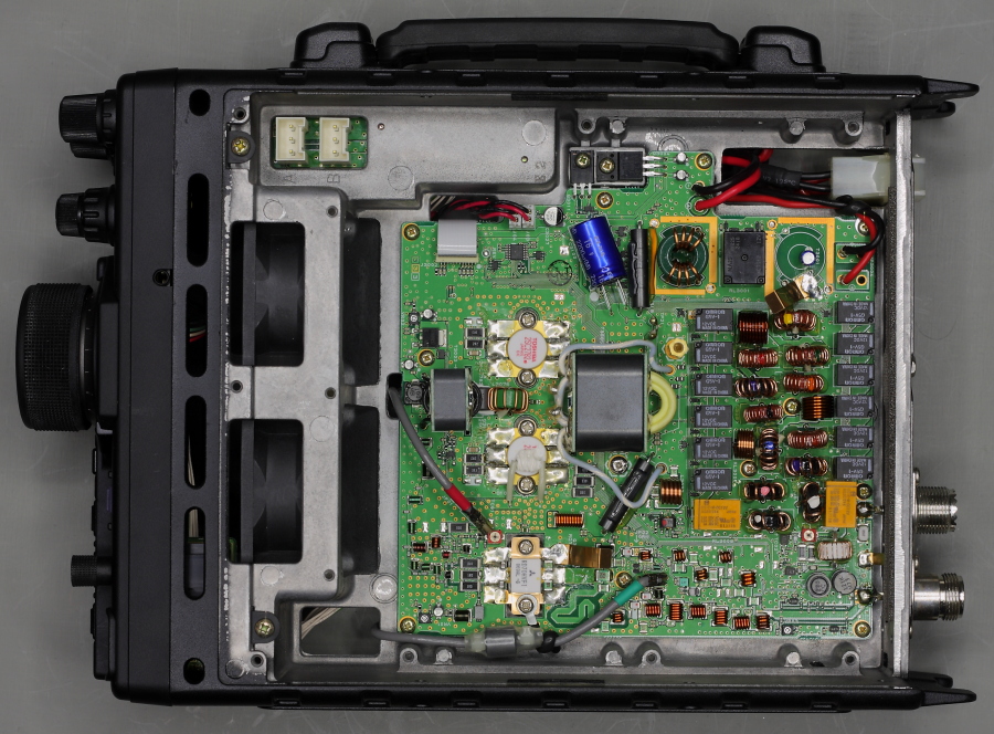
The consists of approximately three printed circuit boards. One PCB behind the front panel, an amplifier PCB with filtering (bottom) and the "mainboard" (top). The CPU and the (pre) driver (s) are placed on this main print. Two FETs are clearly visible in the photo below. These two FETs form a wideband push-pull amplifier that powers the power amplifier. (These two FETs are the output stage in the FT-817.) These two FETs are soldered to a heat sink that is connected to the frame. These FETs are known to fail. Since the FETs are connected directly to the power supply input, they can be exposed to peak voltages that the FETs have poor resistance to. Do not replace these FETs yourself if you are not experienced! Even the most experienced (SMD) soldering artist can go wrong here! The operation can be performed without damage, there is a lack of sufficient knowledge and skills. I have unfortunately seen several battered hoofprints with whole pieces out ... When a hobby Bob has been at work: "Turn around and walk away from the set ...". Fumbling in this area is difficult to repair. Two push-pull transformers are clearly visible before and after the driver FETs. Pre-drivers are placed in front of the driver. Two of these (superimposed) parallel-connected semiconductors can be seen on the right of the photo. These are class-A amplifiers, not in push-pull setup. As a result, the return is lower, but because the capital here is limited, this is not a problem. The other amplifier stages before the pre-driver are placed at the bottom of the PCB. The generated power from the driver goes via the red marked coaxial cable to the output PCB at the bottom of the set.
|
|
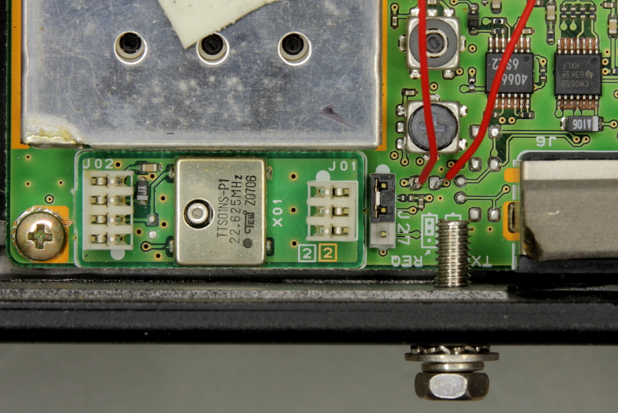
TCXO (FT-897 vs FT-897D)
|
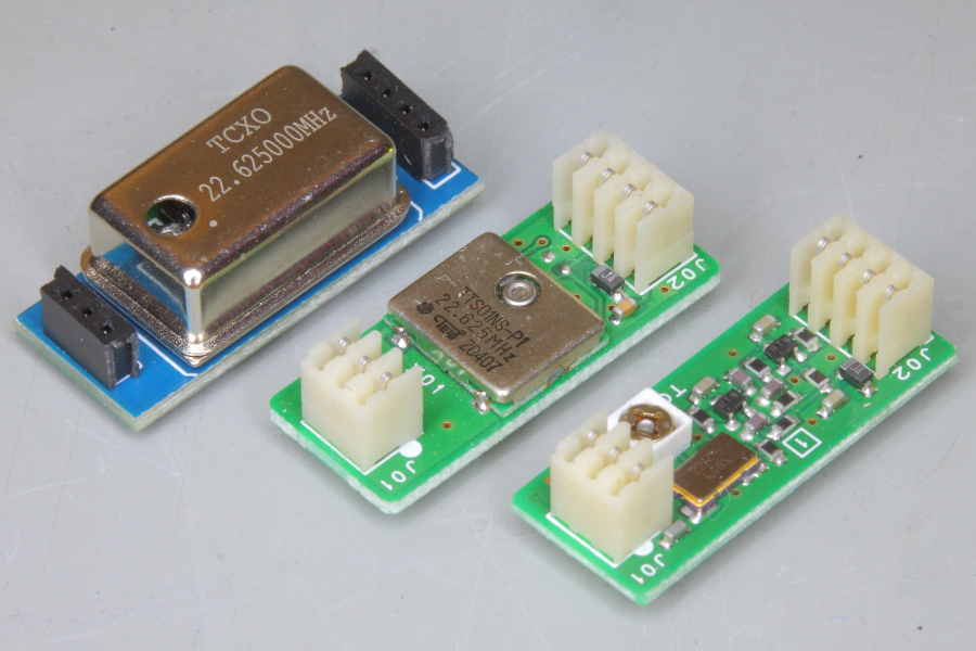
The difference between the FT-897 and the FT-897D is the TXCO option. The FT-897 has no temperature compensated oscillator and the TF-897D sucessor is equipped with an TCXO oscillator. Remind that the “D” is not shown on the front panel. It is said that untill lot number 28 was the TCXO module an option. From lot 29 the TCXO is installed by default for “free”. The original “REF Unit” can be easily replaced by a “TCXO module”. Since the modules are plugin modules, always check if the TCXO is installed insead of checking the lotnumber only. (Digits 3 and 4 of the serial code represent the lotnumber.) The TCXO has a stability of 0.5 ppm. Since it isn't a OCXO, the current consumption is neglectable. The TCXO is placed on the mainboard (underneath the top cover) near the power input connector.
|
|
power amplifier versions
|
|
|
mainboard
|
 old model (lot 1 ~ 68) old model (lot 1 ~ 68)
 new model (lot 69 ~) new model (lot 69 ~)
|
|
power amplifier board
|
Trough the years a series of different batches are produced. Due to improvements the hardware can be differtent per lot / batch. There are serveral (small) changes made during the production period. The only substantial changes are made in the power amplifier board. The output transistors / FET's are replaced (along with some surrounding components). The VHF / UHF transistor has been replaced by a FET. The original output transistor turned out to be not stable enough at high power. This could lead to failure of the power transistor (s). Beware that the newer FET design is different than the older transistor amplifier design and therefore these semiconductiors are not interchangeable! Even the bias currents of the three final amplifiers are changed corresponding to the amplifier semiconductor type. The older design has a bias current of 100/300 mA and in the new design the bias current is 600 / 1,000 mA! Replacing an old type final transitor with a new FET isn't therefore possible! Both of the board types are shown below:
Old PA board lot 1 ~ 68)
Old PA board lot 69 ~)
 new model (lot 69 ~) new model (lot 69 ~)
|
|
transmission power
|
It is possible to get more radio frequency transmission power from the FT-857 (D). My advice is this modification does notbecause the transceiver is not designed for it. In particular, it is not recommended to increase the power of the UHF stage of radios with a lot number up to and including 68. If more power is desired, it is advisable to use an extra power amplifier. The modification for more transmit power can be found here and there and a warning for this seems to me to be in place because carrying out the modification etg is unwise. It provides about 30% more transmit power and provides minimal benefit. It doesn't even save one s point on the receiving end. The warranty will of course expire, but a bigger objection is that the device is not designed for it. The output stage is overloaded and the risk of (irreparable) damage is conceivable.
The HF output stage is calculated at 100 W SSB. It is possible to broadcast on FM, but not conceivable given the band plan. The heat development at SSB on HF is easy to oversee because through speech the power is not continuous and the heat load is therefore not too bad. However, when a digimode such as RTTY or PSK is used, the heat load is almost continuous. The advice is to reduce the power of a digimide in order to maintain the FT-897 output stage. If a PSK31 station with 25 W cannot yet be decoded, it will not go much better with 100 W. Atmospheric conditions are much more important than transmission power.
|
|
User Port switching
|
Alan; 9A6RT found an interesting feature in the FT-897 rig. In the middle of the mainboard five soldering pads are located. The one closest to the rear of the rig is TP1021. The closest to the frontpanel is a ground connection. Alan found out that the 4094 shift register chip outputs can be switched by the software. He discovered two of the pads are switched to 5 VDC when the transverter option is switched on. One pad (TP1023) for transverter "A". And another pad (TP1024) for transverter "B". Therefore it's possible to switch a connected transverter on or off by activating the transverter in menu item # 91. Test point TP1021 is switched to +5 VDC if menu item # 65, 66 or 67 (extended menu set on) is set to USER and activated from the main screen. Maybe this is usable for a built in Tinytrak or other kind of TNC, switch or related device. Remind that the 4094 can handle only a very small amount of current! If you want to drive a relay for example, a switching transistor like a BC517 is needed! It might be an idea to add a led light underneath the rig for logbook lighting in low light conditions switched by the [USER] button. I verified the information on my rig and the information is correct. (The FT-2800M has also this User Port option built in.)
 TP1021 = +5 VDC if menu # 65 (PG1), 66 (PG2) or 67 (PG3) is set to USER and activated from the main screen TP1021 = +5 VDC if menu # 65 (PG1), 66 (PG2) or 67 (PG3) is set to USER and activated from the main screen
TP1022 = unknown
TP1023 = +5 VDC if XVERT A is activated via menu # 91
TP1024 = +5 VDC if XVERT B is activated via menu # 91
ground pad
|
|
flickering squelch problem and solution
|
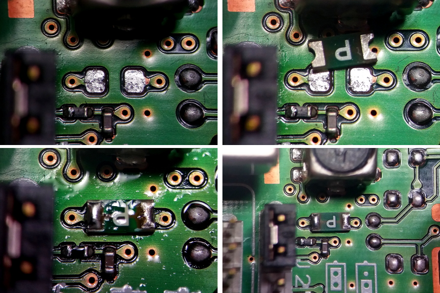
The FT-897 has flickering squelch behavior in standby mode. Even if there's no (weak) signal, the squelch opens for a short amount of time. This flickering is rather anoying and this could be solved by adding a capacitorto the mainboard. I read about this solution described by Jochen; DG2IAQ. Jochen discovered that the original 0.47 uF SMD capacitor is too small for stable squelch operation. SMD capacitor C1336 is marked "E474". To solve the flickering squelch problem, add one 4.7 uF electrolytic capacitor in parallel with existing capacirot C1336. The C1336 capacitor is located between the DATA and ACC connector on top of the mainboad. The negative side is near the back end of the radio. Jochen; DG2IAQ assured 4.7 uF is the right value since he performed several test on this. The squelch should perform much better / sharper, the squelch level is the same as before, weak signals are detected better and more stable and the flickering is gone. So don't worry, no weak signal will be missed. The modification will add some delay after closing the squelch,
I performed the modification as described and I can tell the performance of the rig improved a lot . The squelch is much more stable and I would recommend performing this modification . I made an image of my rig with the added capacitor which is shown above. With some smd soldering skills (and patience), this modification is rather easy. The tricky part is removing the mainboard from the radio. Take your time performing the modification and beware not to damage the white flatcable. Remind that the exciter heatsink and driver requires new thermal paste for conducting heat to the metal housing. If your not familiar with smd soldering or not skilled in this area, maybe [Link: http://www.radioamateurshop.nl]: Radioamateurshop (located in The Netherlands) can help you out. Leo adviced me also to use a SMD capacitor instead of the shown electrolytic capacitor. I haven't upgraded the circuit yet. For now the electrolytic capacitor is doing it's job quite well.
|
|
ACC port TX request (input) or TX ground (output)
|
The ACC connector at the back of the radio has two functions. The ALC (Automatic Level Control) input signal at the tip of the connector for adjusting the signal levels using if a additional power amplifier is used. The ring of the 3.5 mm mini jack connector can be used as a TX request or TX ground as a "second" function. By default it's set as TX request. Therefore the rig wants to transmit if the ring of the connector is connected to ground (connector sleeve). This can be convenient using an aftermarket antenna tuner for sending a steady CW carrier for tuning.
It's possible to change the TX request to TX ground. If so, the ring connection of the 3.5 mm mini jack will be shorted to ground by the rig. This could be convenient using a (not CAT port controlled) power amplifier for switching from receive to transmit (and vice versa).
To change the function of the port, change the jumper position J27. Remove the top cover of the rig and locate the black jumper position J27 near the external ground terminal. The corresponding position is silkscreen marked as TXR (TX request) and TXG (TX ground). Place the jumper as for the desired functionality.
If you like advanced "hacking" it's even possible to remove the jumper and use the center contact for an other signal like an IF output signal. The center contact is connected to the ring of the ACC 3.5 mm mini jack. Se the schematic below for more details.

|
|
J1010 (programming) connector reverse engineering
|
The mainboard of the FT-897 radio is equipped with an "unknown" male white 7-pin conector marked J1010 near to the optional filter positions next to the relay. There's nothing connected to it wich seems odd. Sincs I was digging around in the schematics I spent some time trying to find out the original purpose of this connector and maybe discover a conventient new purpose for it. In the schematic I found the following pin information:
1 = ground
2 = RXD (mic up button)
3 = TXD (mic down button)
4 = ground (for pull down)
5 = +5 VDC (for pull up) (seems not connected ...)
6 = microprocessor reset (when pulled low)
7 = VCC (+13.8 VDC)
One interesting thing it that pin 5 is marked as a +5 VDC signal for pull up purposes, but there's no lead attatched to the pin. The data transmit (TXD), receive (RXD) and reset (RES) are directly connected to the central microprocessor Q1049. According to the datasheet of the HD64F2134ATF20 microprocessor, there are three sets of data busses. One data bus is used for communication between the main unit and panel unit (MP) via cpu pins 11 and 10, one is dedicated fot CAT terminal use via cpu pins 39 and 40 and one is used for CAT purposes via the microphone (MAIN- MIC) using cpu pins 39 and 40. The last mentioned data bus is also connected to the "unknown" J1010 port. Since the port has also a cpu reset pin available, it's likely the J1010 port is used for programming (or debugging) the radio (microprocessor). The reset requires ground to be activated and no pull-up signal is needed. Maybe therefore there isn't a 5 VDC wire connected to the J1010 connector. I can imagine that the J1010 port is used to hook up a programming or testing device during production of the mainboard. Using connector J1010, the cpu can be powered and programmed without any other wire connected to the board (or built into the housing). When the rig is assembled completely the micrphone port can be used for programming or debugging without removing the top panel fot access to the J1010 port. Unless you're in hacking or reverse engineering of microprocessors, I don't thing this port is relevant to use ...
|
|
relay cleaning / testing
|
There is an official undocumented feature built in the FT-897 rig. It's possible to power all the tuner relays individual for cleaning or testing. The official purpose is relay cleaning since the display shows "RELAY CLEANING". But it seems likely that it's more useful for relay testing. If one relay goes bad and gets sticky, this feature lets you determine if all the relays switch as it should. The procedure for testing is this:
Power off the FT-897 if it's turned on;
Press and hold down [UP] and [DOWN] simultanious and then press the [POWER] button;
The rig switches on and the relay cleaning procedure is started. The display is showing "RELAY CLEANING".
The rig is now again ready for use.
|
|
Serial Number
|
The transceiver serial number can be found on the white sticker on the left side of the transceiver. The coding is logically structured and the year of manufacture, month of manufacture, production series (lot number) and serial number can be derived from this. In this example we will take the (fictitious) serial number "4M311234".
The first character is the last digit of the year. In my case, the 4 represents 2004. Note that a "0" represents 2010.
The second character is a letter corresponding to the month where "C" represents January, "D" represents February, and so on. In my case, "E" stands for the month of March.
- I = July
- J = August
- K = September
- L = October
- M = November
- N = December
The next two characters are the lot number. In my case number 31 stands for lot number 31.
The last four characters represent the sequence number per batch, in this fictitious case sequence number 1234.
|
|
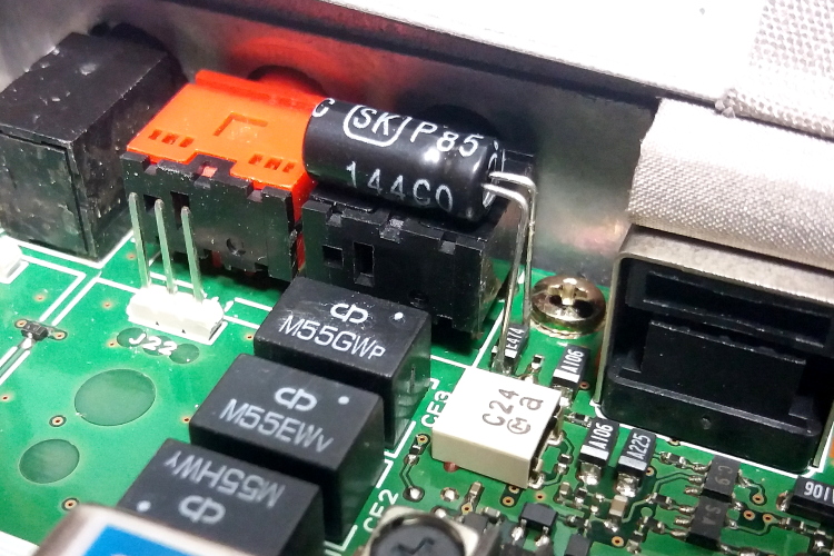
Fuse replacement
|
The first step to do buying a rig is look (and smell) inside the device. That can tell a lot about the history. Burned components can be smelled or be seen. In my case, the first thing I noticed was a "replaced" smd fuse. To see the picture below can be seen how the problem was solved. Two red wires were soldered to the mainboad and to a 5x20 mm fuseholder. The original smd fuse can handle 3.15 A. That's quite an amount of current. I wonder what happened here ... It's obvious the repair is performed rather bad. There's even a piece of toilet paper used to keep the fuseholder in place. Luckily nothing is damaged and everything can be repaired perfectly. (For the record, the replacement fuse could handle a couple of milliamps.)
Well, now the good news. The repair ... I used a stereo microscope to get a clear view to the "broblem area". Using some flux, desoldering wick and a small tip soldering area for claning the pads. With q-tips and some Isopropyl alcohol the board is cleaned up nice. The new 3 Amps (P-marked) smd fuse is placed using patience and tweezers and soldered in place. After soldering the board is cleaned the same way as described above. It's highly unlikely the fuse will be blown again, so an original smd replacement part is fine. Now the rig is back in it's original state. The repair is quite simple if you are experienced with smd soldering and have the proper equipment. You do need a microscope, a small tip soldering iron and very thin soft solder. I wouldn't recomment this as your first smd project.
The original Yaesu components are bought from [Link: http://www.radioamateurshop.nl]: http://www.radioamateurshop.nl. [Link: http://www.radioamateurshop.nl]: Radioamateurshop from Oldebroek (The Netherlands) can also perform the fuse replacement described above.
|
|
Versions / designs
|
Versions
There are two versions of the Yaesu FT-897, namely the FT-897 and the FT-897D . There may be misunderstandings about this, hence a brief explanation:
Both versions have FT-897 on the front, so also the FT-897D;
The type plate says FT-897 or FT-897D, but the version can be derived from this;
All FT-897s have DSP. (With the FT-857 (D) this was an option.)
To my knowledge, all FT-897's with batch number 29 and above are FT-897D;
At batch numbers 28 and below the TCXO was an option and therefore an FT-897.
The only difference is that the FT-897 (not "D") has a "standard oscillator" and the FT-897D has a TCXO.
TCXO
The FT-897D has a TCXO (Temperature Compensated Crystal Oscillator) or reference oscillator that is temperature compensated. An oscillator is subject to frequency fluctuations depending on the temperature. Especially with narrow (CW / digimode) signals, it is desirable for the frequency to be stable because the transmitter and receiver "drifts" from frequency. For wide signals such as FM use, a more stable oscillator is less relevant. A few Hz drift is hardly noticeable. By replacing the "REF UNIT" with a "TCXO UNIT" the upgrade from an FT-897 to the FT-897D has been made. Whether it's an FT-897 or an FT-897D is not a showstopper for purchase . The TCXO is a small plug-on PCB that is easy to replace. TCXOs for sale.
batch number overview
The third and fourth characters of the serial number of an FT-897 (D) together form the batch number / lot number. The batch number is important to be able to judge which hardware version the FT-897 is. It is therefore very important that the correct service data is used during adjustments and repairs, because this is linked to the hardware version. For example, one model has a quiescent current of 1,000 mA in the power amplifier and the other "only" 300 mA. And the correct value must of course be applied to keep the equipment intact.
Several changes have been made to the design for improvement. Most of the changes are minor, insignificant changes. The biggest difference is in the power amplifier. The first generations, batch number 68 and below, have a transistor in the V / UHF output stage. Power amplifier on set with batch number 69 and higher have FETs in the in the power amplifier. Below is an overview of the changes per batch number to give an impression of the changes. Each block is one type of revision.
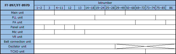
The "old" (batch 68 and earlier) represent a lower market value because the output transistors are of an obsolete model. This may not be a problem, but in the event of failure of an output transistor, replacement could potentially be a problem over time as the components may be more difficult to obtain. I have had several FT-897's, also from a (very) low batch number and never had any problems with it. With good antenna tuning, output stages can last a long time. In case of abuse due to poor adjustment and maximum power on FM / digimode on the HF bands, there is a lot of heat development and wear. When an FT-897 is handled properly, an old model is still fine!
valuation
But it is something to take into account when determining the value when purchasing. Depending on the age, condition, possible defects and the batch number, a fair market value is € 500.00 for a used set. A bare "worn out" FT-897 can sometimes be found under € 400.00 and a recent neat one can still go towards € 600.00. Optional filters have a big impact on the price, as do options such as a built-in power supply and the like. I bought FT-897s for around € 400.00, but then you have to take into account that something is broken such as a display with failure, encoders with a lot of play, broken PIN diodes, bad repairs and the like. In short, if you do not want to gamble, it is better to spend € 100.00 more for a neat good one instead of a craft bin. Always check the transmission power! The push-pull drivers of the output stage sometimes fail. This is clearly noticeable in insufficient transmission power and strongly fluctuating transmission power on all bands. Replacing the two "chips" can only be performed properly with sufficient knowledge and skills! Never underestimate this repair! This tricky operation is not exactly free and has a strong impact on the market value. I once owned and sold a batch 90 FT-897 due to an (hindsight) upgrade to an FT-991. During the sale, it turned out that the driver was malfunctioning. : '- (The buyer is then financially compensated ... can only be done properly with sufficient knowledge and skills! Never underestimate this repair! This tricky operation is not exactly free and has a strong impact on the market value. I once owned and sold a batch 90 FT-897 due to an (hindsight) upgrade to an FT-991. During the sale, it turned out that the driver was malfunctioning. : '- (The buyer is then financially compensated ... can only be done properly with sufficient knowledge and skills! Never underestimate this repair! This tricky operation is not exactly free and has a strong impact on the market value. I once owned and sold a batch 90 FT-897 due to an (hindsight) upgrade to an FT-991. During the sale, it turned out that the driver was malfunctioning. : '- (The buyer is then financially compensated ...
|
|
